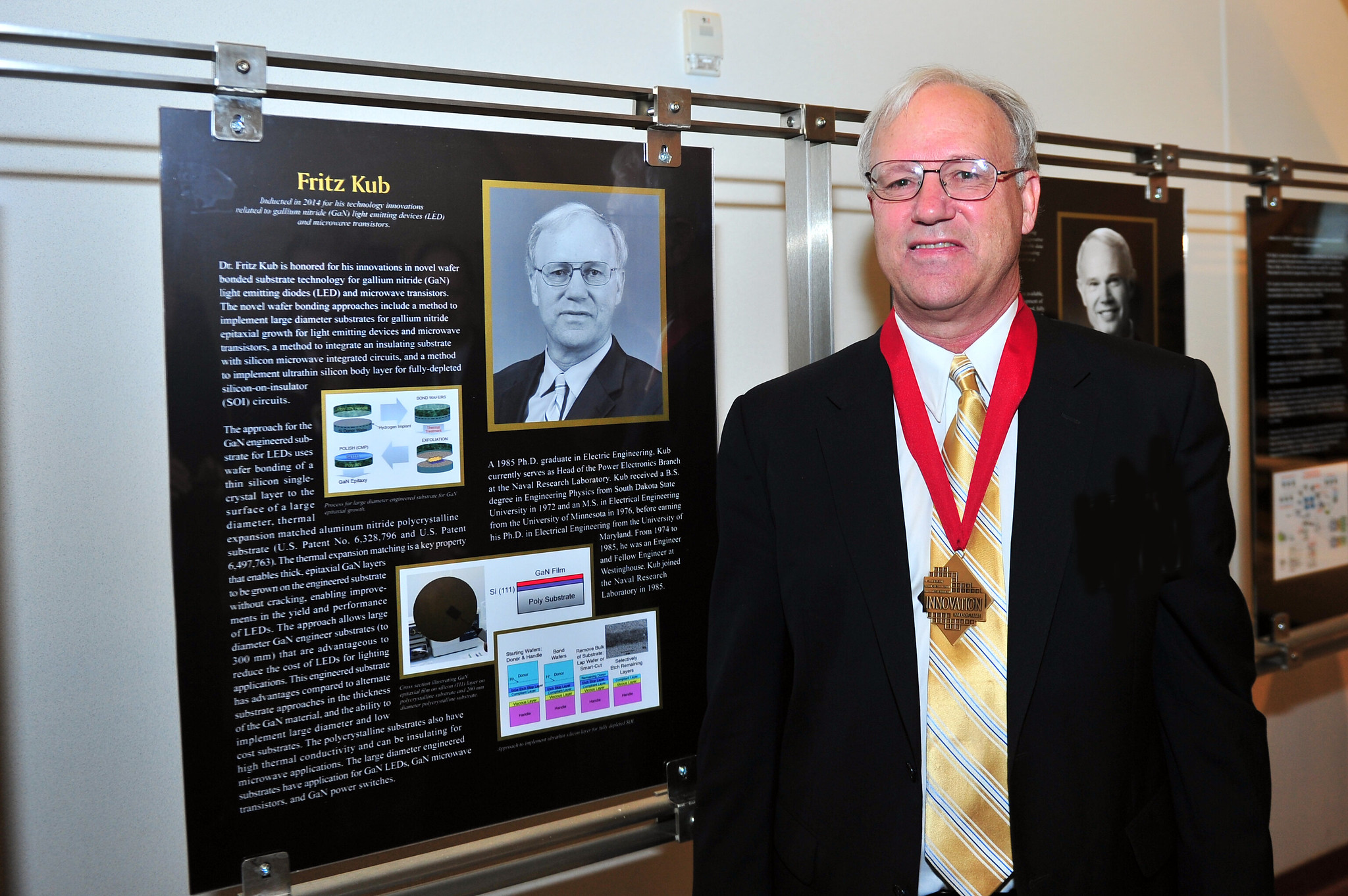
Inducted in 2014 for his technology innovations related to gallium nitride (GaN) light emitting diodes (LED) and microwave transistors.
A 1985 Ph.D. graduate in Electrical Engineering, Kub currently serves as Head of the Power Electronics Branch at the Naval Research Laboratory. His thesis advisor at UMD was Professor Hung C. “Jimmy” Lin (1919-2009), a prolific inventor and university benefactor whose innovative spirit was shared by his former advisee. Lin was awarded more than 60 U.S. patents over the course of his lifetime.
Kub’s innovations in novel wafer bonded substrate technology for GaN LED and microwave transistors include a method to implement large diameter GaN engineered substrates, a process to implement an ultrathin silicon body layer for fully-depleted, strained silicon-on-insulator (SOI) circuits, and a technique to integrate an insulating substrate with silicon microwave integrated circuits.
The approach for the GaN engineered substrate for LEDs uses wafer bonding of a thin silicon single-crystal layer to the surface of a large diameter, thermal expansion matched aluminum nitride polycrystalline substrate. The thermal expansion matching is a key property that enables thick, epitaxial GaN layers to be grown on the engineered substrate without cracking, enabling improvements in the yield and performance of LEDs. The approach allows large diameter GaN engineer substrates (to 300 mm) that are advantageous to reduce the cost of LEDs for lighting applications.
This engineered substrate has advantages compared to alternate substrate approaches in the thickness of the GaN material, and the ability to implement large diameter and low cost substrates. The polycrystalline substrates also have high thermal conductivity and can be insulating for microwave applications. The large diameter engineered substrates have application for GaN LEDs, GaN microwave transistors, and GaN power switches.
Kub received a B.S. degree in Engineering Physics from South Dakota State University in 1972 and an M.S. in Electrical Engineering from the University of Minnesota in 1976, before earning his Ph.D. in Electrical Engineering from the University of Maryland. From 1974 to 1985, he was an Engineer and Fellow Engineer at Westinghouse. Kub joined the Naval Research Laboratory in 1985.
He has played key technical and leadership roles in research and development of microelectronic devices such as: wafer bonded materials and devices, GaN power transistors, integration of diamond with GaN power transistor, silicon carbide power transistors, neutron detectors, and analog CMOS circuits. He has more than 150 journal publications and 52 U.S. patents.
In 2011, Kub was designated a Fellow of the Institute of Electrical and Electronics Engineers (IEEE) and received the Distinguished Engineer Award from South Dakota State University in 2010. He has received two Naval Research Laboratory Best Publication Awards and five Naval Research Laboratory Technology Transfer Awards. He was also co-author on a paper that received the Japan Society of Applied Physics 2014 Outstanding Paper Award and was co-author on a paper that received the Best Poster Paper award for 14th International Conference on Atomic Layer Deposition.
View Photos from krub's Induction CeremonyTop