News Story
QTC-MITRE Collaboration Receives Best Paper Award at EDFAS 2020
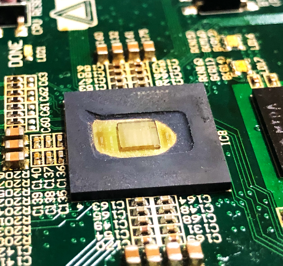
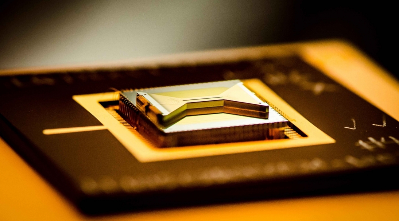
Diamond on top of a decapped integrated circuit.
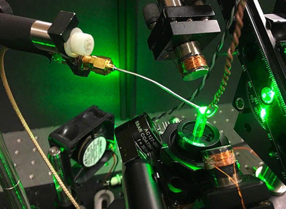
Our increasing reliance on microelectronics in our interconnected world and the rapidly expanding complexity of integrated circuits necessitates further advancements in tools to characterize the security and the performance of these chips. Researchers at the Quantum Technology Center (QTC) at the University of Maryland are collaborating with the MITRE Corporation to develop a new method to peer into the inner workings and function of integrated circuits (IC) using a Quantum Diamond Microscope (QDM) for widefield magnetic imaging.
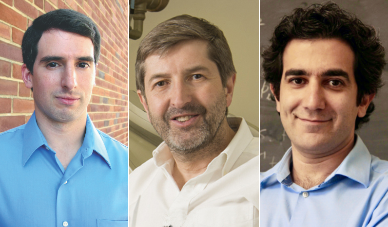
The paper titled “Backside Integrated Circuit Magnetic Field Imaging with a Quantum Diamond Microscope” won the 2020 Best Paper Award at the International Symposium for Testing and Failure Analysis (ISTFA) Workshop held virtually on December 7–9, 2020. The project is funded by MITRE, and the paper was written by Ronald Walsworth, QTC founding director and UMD professor of electrical and computer engineering and physics, Matthew Turner, QTC staff scientist, Edlyn Levine, QTC visiting associate research scientist & chief technologist at MITRE Engenuity and MITRE PI for this work, and Nicholas Langellier, Thomas Babinec, and Marco Lončar of Harvard University.
Their paper, a follow-up to their original work to extend the applicability of the QDM technique to a wider variety of integrated circuits architecture, presents a new method for backside IC magnetic field imaging using QDM nitrogen vacancy magnetometry. They demonstrate the ability to simultaneously image the functional activity of an IC thinned to 12 µm remaining silicon thickness over a wide field of- view (3.7 x 3.7 mm2). This 2D magnetic field mapping enables the localization of functional hot-spots on the die and affords the potential to correlate spatially delocalized transient activity during IC operation that is not possible with scanning magnetic point probes. They use Finite Element Analysis (FEA) modeling to determine the impact and magnitude of measurement artifacts that result from the specific chip package type. These computational results enable optimization of the measurements used to take empirical data yielding magnetic field images that are free of package-specific artifacts. They also use machine learning techniques to scalably classify the activity of the chip using the QDM images and demonstrate this method for a large data set containing images that are not possible to visually classify.
ISTFA’s partnership with the International Symposium on the Physical and Failure Analysis of Integrated Circuits (IPFA) offers the EDFAS Virtual Workshop Best Paper winner to attend and present at IPFA 2021. The authors will receive an award at ISTFA 2021, which will be held October 31–November 4, 2021 in Phoenix, Arizona.
Published June 14, 2021
Related Stories
Stories / June 1, 2021
Quantum Technology Center Adds Three New Fellows

Stories / May 6, 2021
QTC Awarded $1.5M from the Department of Energy for Research on...

Stories / October 11, 2021
Diamonds Are a Quantum Sensing Scientist’s Best Friend
Stories / September 10, 2021
UMD joins NSF-funded revolutionary $25M center for...
Stories / January 21, 2021
Micron-scale NMR Spectroscopy using Diamonds
Stories / August 18, 2020
Gong Paper on Ferroelectric Control of Half-Metallic 2D...
Stories / August 18, 2020
QTC Researchers Combine QDM and ML to Noninvasively Probe an...
Stories / October 4, 2021
Foundational Step Shows Quantum Computers Can Be Better Than...
Stories / September 2, 2021
UMD Leads New $25M NSF Quantum Leap Challenge Institute for...

Stories / June 24, 2021
Hafezi Appointed as Minta Martin Professor of Engineering