Reducing Our Lead Footprint |
|
FOR IMMEDIATE RELEASE CONTACT: Faye Levine
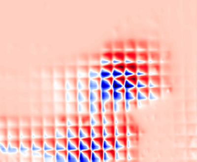
COLLEGE PARK, Md.—Researchers at the University of Maryland's A. James Clark School of Engineering have discovered a new lead-free material, bismuth samarium ferrite (BSFO), for use in products ranging from biomedical imaging devices to airbag sensors to inkjet printers. If implemented commercially, it could replace a common lead-based material found in these and other electronic devices, keeping lead out of landfills and the ecosystem. "One of the reasons it's so hard to let go of lead is because it's so useful," explained Ichiro Takeuchi, associate professor in the Clark School's Department of Materials Science and Engineering. "Its properties make it ideal for use in electronic devices." According to the Environmental Protection Agency, U.S. households threw out more than 300 million electronic devices in 2006, many of which were exported to other countries for recycling, where their lead components were improperly disposed of [1]. When the U.S. moves to digital-only broadcasting in early 2009, thousands of older, lead-containing analog TV sets could end up in landfills around the world as well. While manufacturers have developed replacements for lead in many products, until now no commercial replacement existed for lead zirconate titanate (Pb(Zr,Ti)O3, or PZT)—the material of choice for transducers, actuators, sensors, and microelectromechanical systems used in common electronic devices. PZT is more than 40 percent lead, but it also has piezoelectric properties, which means it acts like a switch—it can either create a voltage when mechanical stress is applied to it, or it can deform its shape when voltage is applied. This behavior is used to create actuators, moving components in electronic devices that translate electrical input into motion to accomplish mechanical tasks, such as controlling the inkjet nozzles on a printer. Takeuchi and his collaborators at the University of Maryland's Keck Laboratory for Combinatorial Nanosynthesis and Multiscale Characterization have created the new piezoelectric material, which in addition to enhanced piezoelectric properties can operate at higher temperatures and is easier to make than other proposed lead-free alternatives. These qualities make it a good candidate for a PZT replacement. The discovery of the new BSFO compound was introduced in a recent issue of Applied Physics Letters. A provisional patent has been filed for the material. Combi—How BSFO Is Made According to Takeuchi, there are only a handful of laboratories capable of this kind of work in the world. The Keck Lab at the University of Maryland is unique among American universities. Takeuchi starts with puck-like pieces of each of his ingredients, in this case bismuth ferrite and samarium ferrite. A precisely controlled laser blasts away molecular sized pieces of each puck, which are then deposited in thin films on a chip. Each film contains varying proportions of the original ingredients. Multiple layers of the films combine to form continuously varying formulae for new materials with new properties, each one just a little different from the next. A collection of these tiny samples housed on a chip is known as a combinatorial library. “In a single experiment, we can study hundreds of different materials,” Takeuchi explained. "You're looking for that perfect combination with the best properties. It's like baking cookies. You want the right proportion of ingredients for the perfect flavor or texture. "You might bake lots of batches of cookies to find the best recipe," Takeuchi continued. "In combi, you're baking a huge number of individual cookies, each with its own recipe, at the same time on the same sheet. In this case, we were looking for something that had piezoelectric properties as good as or better than PZT's." The Best Recipe "A material like this is kind of teetering on the edge," he explained. "It can't make up its mind as to which structure to take. If you apply just a little force or an electric field to it, you suddenly see a huge change. It gets pushed over that edge, the molecular structure rearranges, and the material changes structure. "The ability to snap between these two phases based on external stimulus makes it perfect for use as switches or actuators in electronic devices," he said. "The fact that our version is as responsive as its lead-based counterpart is a huge bonus." The combi technique has shaved years off the research process for Takeuchi's group, he said. "If you made materials like these one by one, you could very easily miss those important phase boundaries," said Takeuchi. "But if you use combi, where one chip contains as many different samples as you want, you can systematically and rapidly measure all of them under the same conditions. Instead of allocating two years to create and test 100 samples one at a time, hoping you find what you're looking for, we can say 'Who cares if it's not there? We made 100 in a day and we can make 100 more tomorrow.'" Although combinatorial synthesis has allowed Takeuchi's research to take a huge step forward, more remains to be done. "Products that use the new compound could hit the market in about five years," he said. "Now that we've discovered it, the next steps are testing it in large scaled-up samples, drumming up industry interest and working out mass production." The lead-free, piezoelectric compound research is currently funded by the Keck Foundation, the National Science Foundation's Materials Research Science and Engineering Center, and the Army Research Office. Takeuchi's collaborators include Clark School of Engineering alumni Shigehiro Fujino and Sung-Hwan Lim; former postdoctoral fellow Makoto Murakami; Clark School materials science and engineering faculty members Manfred Wuttig and Lourdes Salamanca-Riba; University of New South Wales (Australia) faculty Varatharajan Anbusathaiah and Valanoor Nagarajan. References: [1] "Electronic Waste: Harmful U.S. Exports Flow Virtually Unrestricted Because of Minimal EPA Enforcement and Narrow Regulation." United States Government Accountability Office. 17 September 2008. GAO-08-1166T. More Information: About the A. James Clark School of Engineering The Clark School's graduate programs are collectively the fastest rising in the nation. In U.S. News & World Report's annual rating of graduate programs, the school is 17th among public and private programs nationally, 11th among public programs nationally and first among public programs in the mid-Atlantic region. The School offers 13 graduate programs and 12 undergraduate programs, including degree and certification programs tailored for working professionals. The school is home to one of the most vibrant research programs in the country. With major emphasis in key areas such as communications and networking, nanotechnology, bioengineering, reliability engineering, project management, intelligent transportation systems and space robotics, as well as electronic packaging and smart small systems and materials, the Clark School is leading the way toward the next generations of engineering advances. Visit the Clark School homepage at www.eng.umd.edu.
|
|
||||||||||||||||||